Five Gates:
The Day Silicon Learned
to Think in Parallel
A single clock pulse fires. 60 million times per second. An object smaller than a thumbnail resizes the boundaries of human computation.
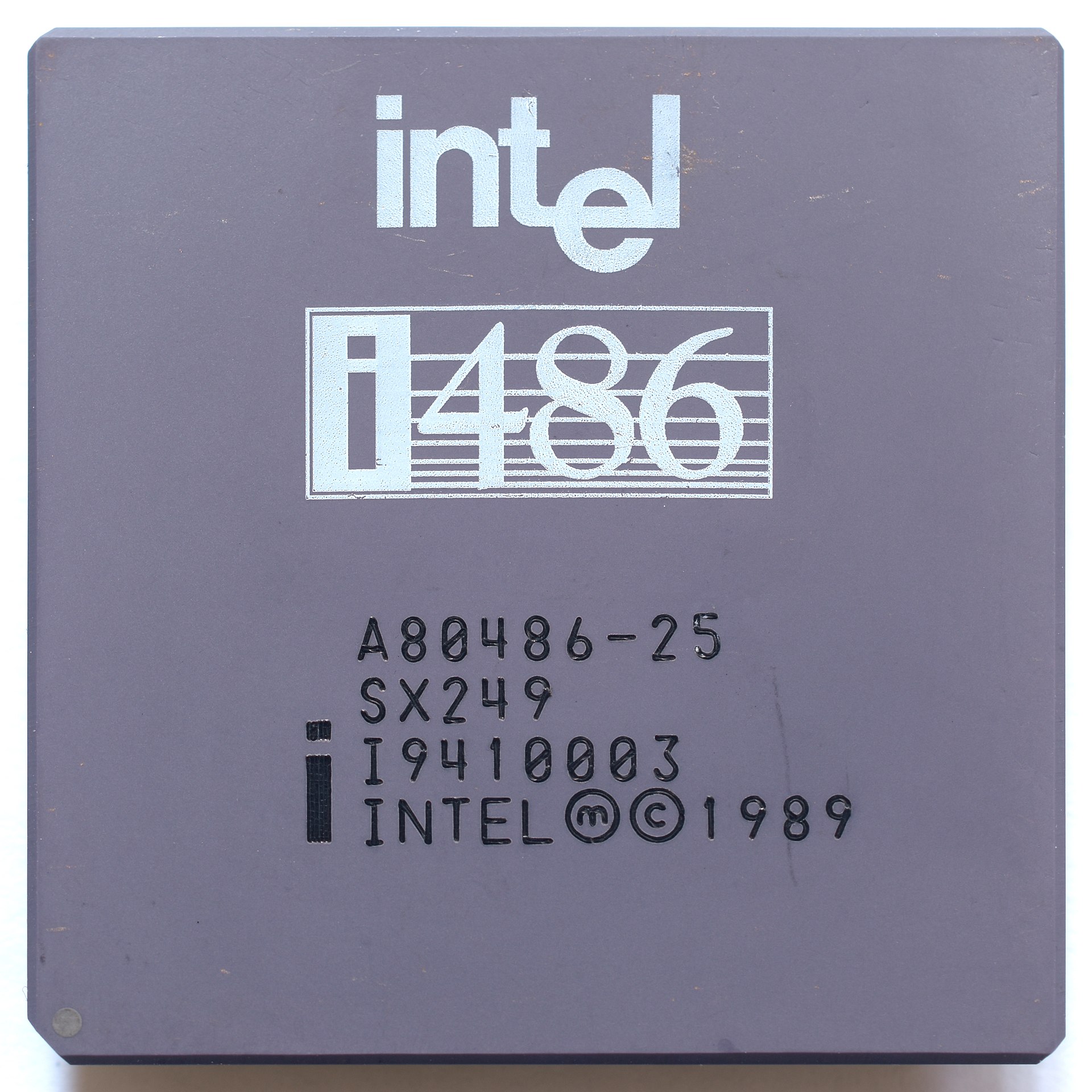
The Intel Pentium processor introduces superscalar architecture—two pipelines running simultaneously through the same microscopic canyon. The sequential era ends. The parallel era begins.
The Architecture
Scroll deeper into the chip. The P5 microarchitecture allowed the processor to execute more than one instruction per clock cycle. Data flows branching along parallel circuit-trace paths, shattering previous execution bottlenecks.
The Acceleration
Generational progression wasn’t just about faster clock speeds; it was about efficiency per cycle. The transition from the 486 to Pentium marked a definitive strobe-like acceleration in processing capabilities.
The Inheritance
What this moment made possible: The sudden viability of CD-ROM multimedia playback. The genesis of unaccelerated early 3D graphics in gaming. The processing headroom required to parse the protocols of the burgeoning internet age. The Pentium didn’t just calculate faster—it opened a door to the modern digital continuum. A spiral of consequence stretching from Santa Clara to every desk on Earth.